
When does semiconductor packaging engineering testing need simulation?
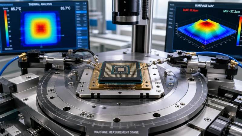
Semiconductor packaging engineering testing needs simulation when the failure mechanism is coupled, slow to emerge, expensive to reproduce, or difficult to isolate with hardware experiments alone. A thermal measurement may show that a package runs hot, but it will not by itself identify whether the dominant cause is die power density, an underperforming thermal interface, a substrate bottleneck, poor heat spreading, or an unrealistic boundary condition. Likewise, a warpage measurement can confirm distortion after reflow, but it cannot efficiently reveal which material layer, cure state, thickness tolerance, or temperature-dependent property is driving it.
The practical question is not whether simulation can replace testing. It cannot. The more useful decision is whether simulation can reduce the number of physical builds needed to reach a defensible design and qualification decision. It is most valuable when it is used before a high-cost prototype loop, during a design or material change, or when test results show a symptom without a clear root cause.
Use simulation when physical testing is too late to influence the design
Many packaging failures become visible only after tooling, assembly, or reliability test vehicles are already in place. At that stage, a redesign can affect substrate procurement, mold tooling, test schedules, customer samples, and qualification plans. Simulation has its strongest project value before those commitments become difficult to reverse.
This is especially relevant where package geometry and material selection are still open: die thickness, mold compound selection, lid design, thermal interface material, substrate stack-up, copper balance, ball pattern, stiffeners, underfill, and package-to-board architecture. A calibrated model can compare options before each alternative requires a separate build.
Simulation should be considered a required engineering workstream, rather than an optional analysis, when a package combines several of the following conditions:
- large die size, thin die, multiple dies, stacked dies, or heterogeneous chiplets;
- fine-pitch interconnects with limited tolerance for differential movement;
- high power density or localized hot spots;
- large differences in coefficient of thermal expansion between adjacent materials;
- high-temperature assembly processes or multiple reflow exposures;
- new mold compounds, substrates, underfills, dielectrics, or thermal materials;
- automotive, industrial, aerospace, medical, or other applications with demanding mission profiles;
- a package revision that must preserve an existing qualification or customer release schedule.
These conditions do not guarantee failure. They increase the number of interacting variables, which makes a trial-and-error build strategy inefficient and makes single-factor conclusions from test data unreliable.
Thermal simulation is needed when temperature measurements do not answer the design question
Thermal testing remains essential, but measured junction or case temperature is an outcome, not a full explanation. A package may pass a simple steady-state thermal check while still developing local temperature gradients that affect solder fatigue, dielectric reliability, timing behavior, or neighboring die performance. This distinction matters in advanced packages because average temperature can conceal concentrated thermal resistance paths.
Thermal simulation becomes necessary when the engineering decision concerns heat flow architecture rather than only compliance with a temperature limit. Typical questions include whether a heat spreader improves the right region of the package, whether a thicker copper layer creates enough benefit to justify substrate complexity, whether an interface material is sensitive to bond-line thickness, and whether a cooling solution remains adequate under nonuniform power maps.
For meaningful results, the model must represent the actual heat path: die attach, interconnect layers, substrate metals and dielectrics, mold compound, lid or heat spreader, thermal interface material, board, and the external cooling boundary. Simplifying these elements may be suitable for early screening, but not for a release decision. An assumed convection coefficient or idealized heat sink contact can make a model look precise while masking the condition that governs field performance.
Transient thermal analysis is particularly important when duty cycles matter. A package used in pulsed computing, power conversion, radar, sensing, or high-speed communications may see repeated temperature excursions rather than a stable thermal state. The amplitude and rate of those cycles influence thermomechanical strain. A steady-state result alone cannot establish whether the chosen package architecture is robust.
Warpage and stress need simulation before reflow and qualification reveal the consequences
Warpage is one of the clearest cases where simulation can protect schedule. It originates from thermal expansion mismatch, cure shrinkage, moisture effects, asymmetric layer construction, die placement, copper distribution, and temperature-dependent material behavior. Physical warpage measurements remain indispensable, but a measurement taken after assembly only indicates the net response of the completed structure.
Finite element analysis can show where the neutral axis shifts, which layers dominate bending, how the package changes shape across the reflow temperature profile, and whether the critical condition occurs at room temperature, peak reflow temperature, or during cool-down. This enables design teams to assess options such as substrate thickness changes, mold compound modulus, die thinning, copper balancing, stiffener placement, or changes to the cure process without waiting for multiple fabrication cycles.
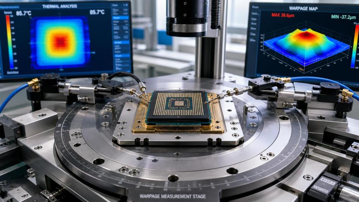
The important point is that a room-temperature warpage number is not always the governing metric. A package that appears acceptably flat at room temperature may warp excessively at elevated temperature, reducing solder joint coplanarity or causing assembly yield loss. Conversely, an elevated-temperature simulation that ignores the package’s post-cure material state may overstate or misrepresent the issue. The temperature range and material state used in the model must match the process or reliability event being evaluated.
Mechanical simulation is also warranted when stress-sensitive structures are present: low-k dielectrics, thin redistribution layers, large silicon interposers, glass elements, fragile passivation structures, dense bump arrays, or die stacks with dissimilar materials. The relevant output is rarely a single “maximum stress” value. A useful analysis identifies stress location, stress direction, temperature condition, time dependence, and the material or interface limit that makes the result actionable.
Do not rely on simplified electrical checks for high-speed package decisions
Electrical simulation is needed when the package is part of the signal path rather than a passive enclosure. At high data rates, package traces, vias, redistribution layers, bumps, balls, planes, decoupling structures, and the printed circuit board interact as one electrical system. Package parasitics can influence insertion loss, return loss, crosstalk, impedance discontinuities, simultaneous switching noise, and power integrity.
Physical measurements on test structures are valuable, but they tend to arrive after layout and fabrication choices have already narrowed. Electromagnetic and circuit-level simulation should be applied when selecting routing topology, reference planes, via transitions, bump assignment, power-delivery arrangements, or decoupling placement. This is particularly important when a package has multiple high-speed interfaces, large die-to-die traffic, sensitive analog sections, or mixed power domains.
A common mistake is to analyze signal integrity and thermal-mechanical reliability as separate tasks with no shared assumptions. In practice, temperature affects conductor resistance and dielectric properties; package deformation can affect interconnect behavior; power-delivery losses add heat; and a revised substrate stack-up may alter both impedance and warpage. Not every program requires a fully coupled multiphysics model, but the interfaces between disciplines must be managed deliberately. Otherwise, one optimization can create a problem in another domain.
Simulation is essential when a material or supplier change is proposed
Material substitutions frequently appear manageable because the replacement meets a nominal datasheet property or has similar chemistry. Packaging performance, however, depends on property combinations across temperature, time, moisture state, and cure condition. A mold compound with a comparable coefficient of thermal expansion may have a different modulus profile. A thermal interface material with similar bulk conductivity may behave differently at the intended bond-line thickness. A substrate dielectric change can affect both mechanical response and high-frequency electrical loss.
When a change is driven by supply continuity, cost, regional sourcing, environmental requirements, or formulation availability, simulation provides a structured way to decide which differences deserve physical qualification attention. It should not be used to declare a substitute qualified on its own. Its proper role is to screen risk, identify worst-case operating conditions, refine the test vehicle, and explain why a proposed change may require broader validation than a basic incoming-material comparison suggests.
The material data package determines whether this exercise is credible. For structural and warpage analysis, relevant inputs may include temperature-dependent elastic modulus, Poisson’s ratio, coefficient of thermal expansion, glass transition behavior, cure shrinkage, viscoelastic response, moisture expansion, and thickness variation. For thermal work, bulk conductivity alone is insufficient when contact resistance or interfacial voiding controls performance. For electrical work, dielectric constant, loss tangent, conductor roughness, geometry, and frequency dependence may be material to the result.
Qualification planning benefits when simulation defines the likely failure window
Reliability testing is often constrained by limited samples, long test durations, and competing program milestones. Simulation cannot replace JEDEC-based or customer-specific qualification requirements, nor can it prove lifetime without validation. It can, however, improve the quality of the qualification plan.
For example, thermomechanical modeling can identify which interface is likely to experience the highest cyclic strain during temperature cycling. Moisture and stress analysis can indicate whether a package is more sensitive during reflow than during storage. Thermal modeling can show whether a power cycling condition produces a larger die-to-package gradient than an ambient temperature cycle. These insights help connect the test condition to the intended failure mechanism.
Without that connection, teams risk running a standard set of tests that consume time but provide limited evidence about the actual design concern. The issue is not that standardized tests lack value; they provide common reliability screens. The issue is that a new architecture, altered material set, or unusual operating profile may have a dominant mechanism that is not adequately explained by a pass/fail result alone.
When simulation adds little value
Simulation is not automatically justified for every semiconductor packaging engineering testing task. A mature, previously qualified package with unchanged materials, geometry, assembly route, power profile, and application environment may gain little from a new detailed model. Likewise, simulation is a poor investment when the input data are unknown and cannot be obtained within the project timeframe. A sophisticated model built from nominal or assumed properties can create false confidence.
It also adds limited value when the immediate issue is a straightforward process-control problem that can be resolved through measurement: a clearly misaligned placement tool, an identifiable contamination event, or a test-handler calibration error. Modeling should answer a decision that physical observation cannot answer efficiently.
The warning sign is a simulation request framed only as “run analysis.” A productive request defines the decision at stake: select between two substrate stack-ups, establish a die thickness limit, determine whether a new underfill changes corner fatigue risk, set an acceptable thermal interface thickness range, or understand why a package passes room-temperature inspection but fails during board assembly.
How to make simulation usable within a project schedule
The first model does not need to represent every microscopic detail. Early project models should be fast enough to compare architecture choices and identify sensitive variables. Higher-fidelity local models are then reserved for areas where the screening analysis indicates meaningful risk: die corners, bump arrays, vias, mold-substrate interfaces, lid corners, or specific hot spots. This staged approach avoids spending weeks refining features that do not affect the decision.
Validation must be planned from the beginning. Model outputs should be compared with available measurements such as warpage profiles, thermal resistance, strain data, electrical measurements, cross-sections, or failure-analysis observations. When results differ, the response should not be to adjust the model until it agrees. The discrepancy may expose an incorrect boundary condition, incomplete material data, unmodeled process variation, or a failure mechanism outside the model’s scope.
Clear ownership is equally important. Package design, materials, assembly, board, reliability, and test functions often supply different assumptions. If those assumptions are not documented, teams may compare results generated with inconsistent power maps, reflow profiles, material states, or mounting conditions. A simulation result is only traceable when its geometry revision, material dataset, boundary conditions, solver settings, and acceptance logic are controlled alongside the hardware revision.
The best trigger for simulation is not the availability of a tool. It is the presence of an expensive uncertainty: a design choice that cannot be judged confidently through simplified calculation or a single physical test. In those situations, simulation turns semiconductor packaging engineering testing from a late confirmation activity into an evidence-based way to choose what to build, what to test, and where the real reliability risk resides.
Recommended News
- 2026.09.14Gel Battery Electrolytes: How Ionic Conductivity and Stability Shape Cell DesignElectrochemistry Fellow
- 2026.09.13Fluoropolymer Extrusion Process: How Melt Control Affects Tube QualityPolymer Synthesis Expert
- 2026.09.12How German Implant Makers Select Medical Polymers for Long-Term BiocompatibilityPolymer Synthesis Expert
The VitalSync Intelligence Brief
Receive daily deep-dives into MedTech innovations and regulatory shifts.