
What should a semiconductor packaging quality test measure?
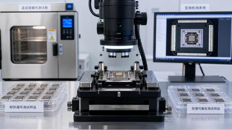
A semiconductor package can look flawless at final inspection and still fail after a few temperature cycles, a humid warehouse transfer, a board-level soldering operation, or months of field use. That is why a semiconductor packaging quality test must measure far more than marking legibility, lead coplanarity, or basic electrical continuity.
For quality-control and safety teams, the real question is whether the package will continue to protect the die and maintain reliable electrical connections under the conditions it will actually encounter. A meaningful test program examines thermal, mechanical, electrical, environmental, and material-related risks together. It should reveal moisture sensitivity, contamination, delamination, cracking, corrosion, warpage, and interconnect degradation before those defects become yield losses, customer returns, or safety incidents.
The exact test plan depends on package type, end use, qualification stage, and customer requirements. Still, the measurement categories below form the practical foundation of a robust semiconductor packaging quality test.
Start with the package’s real failure mechanisms
A package is not merely a housing around a silicon die. It is a layered system of die attach material, wire bonds or bump interconnects, mold compound or lid materials, substrates, redistribution layers, solder balls, leads, and protective finishes. These materials expand, absorb moisture, conduct heat, and react to stress at different rates.
Quality testing should therefore be built around failure mechanisms, not around a generic checklist. A thin quad flat no-lead package, for example, may be especially sensitive to moisture-driven delamination and board-level solder fatigue. A flip-chip BGA may require closer attention to underfill integrity, bump reliability, substrate warpage, and thermal cycling performance. Power modules introduce another level of concern: thermal resistance, high-voltage isolation, partial discharge risk, and long-term degradation under repeated high-current loading.
Before selecting methods, the quality team should define four things clearly:
- The package construction and material stack-up
- The expected assembly, storage, transport, and operating environment
- The critical-to-quality characteristics that affect device function and safety
- The acceptance criteria, sampling logic, and escalation path for abnormal findings
Without this context, testing may generate many reports while missing the risks that matter most.
What a semiconductor packaging quality test should measure
1. Visual condition, dimensions, and package geometry
Visual inspection remains necessary, but it should be treated as an entry point rather than a final decision. Inspectors should look for mold flash, void indications, damaged corners, exposed metal, lead deformation, ball damage, marking defects, contamination, discoloration, and evidence of poor handling.
Dimensional measurements verify that the package fits downstream assembly requirements. Key checks may include body length and width, thickness, lead pitch, standoff height, ball diameter, ball position, coplanarity, warpage, and substrate flatness. Even a small geometry deviation can affect solder-joint formation, automated placement, thermal contact, or mechanical clearance in a compact electronic assembly.
Measurement-system capability matters here. A gauge that cannot reliably distinguish between normal variation and an actual drift creates false alarms in one direction and escaped defects in the other. Calibration status, repeatability, reproducibility, lighting conditions, and operator training should all be controlled.
2. Internal structure and assembly integrity
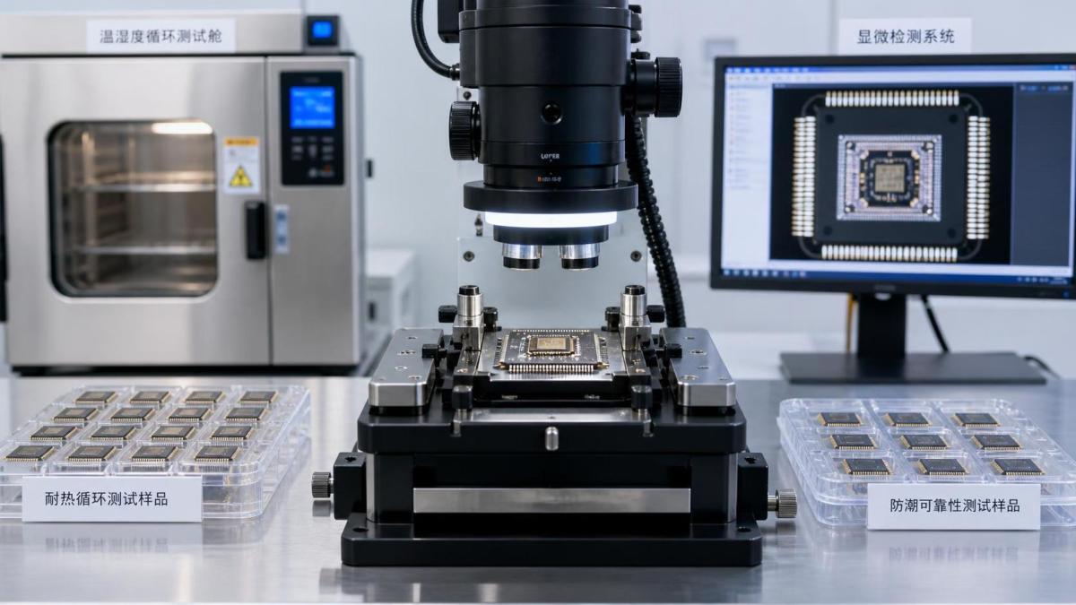
The most consequential defects are often hidden. X-ray inspection, scanning acoustic microscopy, cross-sectioning, optical microscopy, and other non-destructive or destructive methods help determine whether the internal package construction matches the approved design.
Depending on the package, the test should assess:
- Die attach coverage, voiding, thickness, and die placement
- Wire-bond position, loop profile, bond quality, heel integrity, and wire sweep
- Solder bump or ball alignment, voiding, bridging, and collapse behavior
- Underfill distribution and cure integrity
- Mold compound coverage and exposed die-paddle areas
- Substrate traces, vias, redistribution layers, and interconnect alignment
- Cracks, delamination, internal corrosion, and foreign particles
Scanning acoustic microscopy is particularly valuable for detecting delamination at interfaces that may not be visible by X-ray. Delamination between mold compound and die, die attach and leadframe, or underfill and substrate can become a pathway for moisture ingress and stress concentration. The image alone is not enough; teams need defined interpretation rules and comparison against known-good package structures.
3. Electrical performance before and after stress
A package can pass a continuity test while already containing a weak interconnect. Electrical verification should therefore include baseline testing and repeat testing after environmental or mechanical stress. The goal is to detect parametric drift, intermittent behavior, leakage, opens, shorts, and degraded signal or power performance.
The test content depends on device category, but may include continuity, insulation resistance, leakage current, threshold characteristics, functional testing, timing behavior, impedance, contact resistance, and high-voltage performance. For RF, high-speed, sensor, and power devices, package effects on signal integrity, thermal behavior, and electrical isolation may be central to acceptance.
When failures appear after stress, the investigation should not stop at “electrical fail.” Correlating electrical data with lot history, material batches, assembly conditions, acoustic images, X-ray results, and decapsulation findings is what turns a failure into a useful corrective action.
4. Moisture sensitivity and resistance to solder reflow stress
Moisture is one of the most persistent risks in plastic-encapsulated semiconductor devices. Many polymer materials absorb moisture during storage. When the package experiences rapid heating during reflow, absorbed moisture can vaporize and create internal pressure. The result may be package cracking, “popcorning,” delamination, or damage to wire bonds and die attach interfaces.
A semiconductor packaging quality test should verify moisture sensitivity classification and associated handling controls. This commonly involves controlled preconditioning, moisture soak exposure, and simulated solder reflow, followed by electrical testing and internal inspection. Storage labels, dry-pack procedures, humidity indicator cards, desiccant controls, floor-life management, and bake instructions must align with the package’s validated moisture sensitivity level.
For quality and safety managers, this is not a paperwork detail. Inadequate moisture control can cause latent failures that are difficult to trace once components have entered board assembly. It can also create avoidable handling risks where high-temperature processing meets compromised packaging materials.
5. Thermal cycling, thermal shock, and heat dissipation
Temperature changes place repeated strain on every material interface because silicon, metal, ceramics, substrates, mold compounds, and solder alloys have different coefficients of thermal expansion. A package may survive one excursion yet degrade gradually through repeated cycling.
Thermal cycling tests measure resistance to controlled low-to-high temperature transitions over defined cycles. Thermal shock uses more abrupt transfer conditions and can expose weak interfaces rapidly. These tests are especially relevant for automotive electronics, industrial controls, aerospace systems, outdoor infrastructure, power conversion, and devices mounted near heat-generating components.
After stress, teams should look beyond simple pass/fail electrical results. Warpage, cracks, solder-ball fatigue, wire-bond damage, die-attach separation, and changes in thermal resistance may signal an emerging reliability problem. For high-power packages, thermal characterization is critical: excessive junction-to-case or junction-to-board thermal resistance can shorten device life even when electrical parameters initially remain within specification.
6. Mechanical robustness and board-level reliability
Handling, shipping, pick-and-place operations, board flexure, vibration, shock, and connector mating forces can all challenge package integrity. Mechanical test selection should reflect the package’s journey, not just the factory environment.
Common evaluations include lead pull or bend testing, ball shear, ball pull, wire pull, wire bond shear, die shear, mechanical shock, vibration, drop testing, and board-level bend testing. The objective is to confirm that attachment systems have adequate strength and that stress is not transferred into fragile internal structures.
For bottom-terminated and area-array packages, board-level reliability deserves particular attention. A component can leave the package assembly line in acceptable condition but fail later because solder joints are vulnerable to flexing in the final product. This distinction is important when assigning responsibility between package suppliers, contract manufacturers, and OEM assembly operations.
7. Environmental resistance, corrosion, and contamination control
Humidity, corrosive gases, ionic residues, particles, and chemical residues can undermine package reliability over time. Environmental testing may include temperature-humidity bias, high-temperature storage, unbiased humidity exposure, salt or mixed-gas testing where the application requires it, and corrosion assessment of leads, finishes, and exposed metal surfaces.
Contamination control is equally important. Ionic contamination can support electrochemical migration, while particles and organic residues can interfere with die attach, wire bonding, underfill adhesion, or final assembly. Materials entering the package line—mold compounds, epoxies, leadframes, substrates, plating chemicals, solvents, and gases—need lot traceability and incoming-quality controls appropriate to their risk.
Where high-purity chemical systems are involved, supplier documentation should be supported by verification plans. Certificates of analysis are useful, but they do not replace process monitoring, contamination investigation, or disciplined change control.
Standards provide a framework, not a substitute for engineering judgment
Many organizations base package qualification and reliability plans on recognized frameworks such as JEDEC methods for moisture sensitivity, thermal cycling, high-temperature storage, temperature-humidity bias, and solder reflow preconditioning. IPC guidance can be relevant for assembly workmanship, solder-joint evaluation, and board-level processes. Automotive programs may draw on AEC-Q requirements, while military, aerospace, medical, or industrial markets can impose additional customer-specific requirements.
The important point is to apply the right standard version and test condition to the actual package and intended environment. A standard test sequence should not be copied blindly from an unrelated device family. Quality documentation should identify the method used, sample population, preconditioning status, stress conditions, interim read points, failure criteria, and any deviations approved through formal review.
How to interpret results without creating false confidence
Passing qualification does not mean every future lot is automatically safe. Qualification demonstrates that a defined design and process can meet stated conditions. Ongoing production quality requires control plans, statistical monitoring, material-change review, equipment maintenance, operator discipline, and traceability from incoming materials through final shipment.
Watch for trends that remain inside the specification limit but move consistently in one direction: rising die-attach voiding, increased substrate warpage, a shift in wire-pull distributions, more acoustic indications near a particular interface, or a gradual rise in leakage after humidity exposure. These are often early warnings rather than isolated noise.
Likewise, a failure analysis should separate symptom from cause. A cracked mold compound may be associated with reflow stress, but the root cause could be incorrect moisture exposure, an altered mold-compound formulation, insufficient cure, poor die-attach geometry, or transport damage. Containment actions are necessary; process learning is what prevents recurrence.
A practical release checklist for quality and safety teams
Before approving a semiconductor package for production release, supplier qualification, or use in a safety-sensitive product, ask whether the evidence covers the complete risk picture:
- Are package dimensions, markings, coplanarity, and warpage within controlled limits?
- Has internal integrity been verified through suitable imaging and failure-analysis methods?
- Were electrical parameters measured before and after relevant stress testing?
- Is moisture sensitivity defined, and are dry-pack, floor-life, and reflow controls practical for the receiving site?
- Do thermal, mechanical, humidity, and corrosion tests represent the expected service environment?
- Are critical material suppliers, purity requirements, and process changes traceable?
- Is there a documented response plan for abnormal trends, customer complaints, and suspected field failures?
A well-designed semiconductor packaging quality test does not simply decide whether a lot can ship. It creates evidence that the package can protect a device through assembly, transport, operation, and aging. For teams responsible for quality and safety, that evidence is the difference between a component that merely passes inspection and one that can be trusted in the system where it ultimately matters.
Recommended News
- 2026.09.14Gel Battery Electrolytes: How Ionic Conductivity and Stability Shape Cell DesignElectrochemistry Fellow
- 2026.09.13Fluoropolymer Extrusion Process: How Melt Control Affects Tube QualityPolymer Synthesis Expert
- 2026.09.12How German Implant Makers Select Medical Polymers for Long-Term BiocompatibilityPolymer Synthesis Expert
The VitalSync Intelligence Brief
Receive daily deep-dives into MedTech innovations and regulatory shifts.